
SEMICON Japan 2025 live: Researchers introduce nanoparticle tech for advanced packaging
Key takeaways
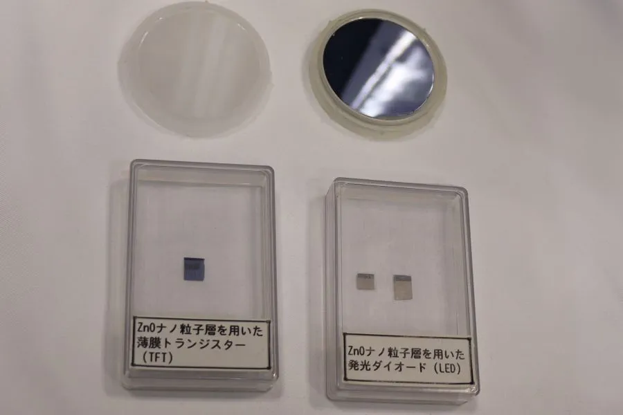
- At SEMICON Japan 2025, researchers from Shimane University’s Fujita–Yoshida Laboratory are presenting semiconductor nanoparticle-coated films.
- The technology can be applied to transparent conductive films, which are used in devices such as optoelectronic chip packages, antennas, RFID elements, and sensors.
- The solution offers a new approach to advanced semiconductor packaging, improving device performance at interfaces.
 Yasuhisa Fujita, professor from the graduate school of natural science and technology at Shimane University
At SEMICON Japan 2025, researchers from the country’s Shimane University’s Fujita–Yoshida Laboratory are showcasing semiconductor nanoparticle-coated films with a single-crystal internal structure.
At the event, we speak to professor Yasuhisa Fujita from the graduate school of natural science and technology at Shimane University to learn more about the latest film innovations and how these can be applied to advanced semiconductor packaging.
The lab, which received the Academia Award 2025 at the trade show, introduces devices built from zinc oxide (ZnO) nanoparticles that can be fabricated by a simple process of coating in the atmosphere. The technology for the growth of ZnO films can be applied to advanced semiconductor packaging.

The solution is suitable for devices using transparent conductive films. Transparent conductive films can be used as transparent electrodes and interconnects in advanced optoelectronic chip packages. Moreover, transparent conductive films can be found in transparent antennas, RFID elements, and sensors.
Fujita tells Packaging Insights on the show floor: “In nanoparticle devices, even with equivalent light-emitting characteristics, achieving high density is difficult compared to single-crystal chip technology due to the effects of interfaces and surfaces.”
“Conversely, by dispersing and coating the material, energy density can be reduced, mitigating the impact of chip heat generation. Therefore, this technology operates in the opposite direction to advanced packaging techniques that integrate chips.”
 The conductivity control technology for these semiconductors enhances photocatalytic properties.Promising material
Shimane University has produced ZnO thin films using metal-organic chemical vapor deposition equipment. The innovation has been commercialized, and a university spin-off company is currently marketing them as high-speed phosphors.
The use of ZnO film in advanced semiconductor packaging is research‑oriented. It aims to improve performance at interfaces or enable novel device features.
“This comprehensive approach — the technological innovation and breadth, commitment to social implementation, and the international education — was highly evaluated,” shares Fujita.
“While most semiconductor devices to date rely on bulk or thin-film single-crystal technology, this technology eliminates the need for single-crystal substrates because luminescence occurs within the nanoparticles, reducing the cost of the semiconductor portion to approximately one ten-thousandth.”
“Furthermore, being an oxide, it does not require the vacuum processes typical of conventional semiconductors. Instead, it enables a cooking-like process: mixing, coating, and baking in air. These developments have the potential to be disruptive innovations in semiconductor devices and semiconductor processes.”